In the world of science I have come to learn that with every small step forward you gain a tool or skill that will make research easier and more efficient in the future. At times I feel like I'm not really moving forward, but then I remember that a marathon is not completed in a single event but many steps. Lately I have had two small victories in the areas of E-beam lithography and AFM. The first is that upon completion of a metal life-off procedure the lines created in the PMMA are actually 20 nm or less! Images of these lift-offs can be seen in Figures 1 and 3. The problem that we continue to battle is that the side walls are not straight up and down vertical but at a slant. At TU last week I used a much shorter development time which lead to the very small metal lift-off lines. When the PMMA was viewed in the SEM, however, it was seen to be continuously pulling away (trenches were widening) due to beam damage.
This raises the question of whether or not we have actually been reaching the small line widths before and the SEM viewing was distorting the PMMA or if they were wide and then viewed. I believe the latter to be true because this was the first instance where the PMMA was seen to be actively moving under the electron beam, whereas before it had already moved and was then viewed. I think that the longer development times overdeveloped the walls, causing the slant, which were then viewed under SEM and did not move because they had already reached their "equilibrium" position. So when the development time was shortened only the exposed area was developed and upon viewing the PMMA began shifting to its equilibrium position and we were able to see it.
Another question that arises is how it the beam damage occurring if we are sputtering with gold? Two possibilities is that the gold layer is not thick enough (roughly 2.5 nm on the surface may not be enough to negate the effects of the beam) or perhaps the side walls of the trench were not coated because they were straight up and down. If this were the case if could also explain why the overdeveloped slanted walls did not move when viewed. Because they were already slanted the gold formed a layer there which could have helped protect against beam damage. The straight vertical walls may not be coated as well and therefore when viewed under SEM they are not protected and experience the beam damage. This theory will be checked using a rotating thermal evaporator in an attempt to coat the side walls of an un-viewed sample, and it will then be viewed to see if the same damaged and extreme movement occurs again.
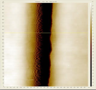
The second small victory is the use of high-resolution AFM probes in order to see the bottom of one of our trenches and make a more accurate measurement. The cross sectional view of such a trench can be seen in Figure 4. As compared with the last post in which the trench was roughly measured as 300 nm across and "V" shaped, this new measurement shows a trench with a square bottom. The slanted walls are still present, and show some tip-sample interaction on the left side of the cross section which is still being investigated, but the sample bottom appears to be roughly 58 nm across. The sample used was an older one with many doses being tested and it is difficult to know which dosage this was but due to the recent success with the metal lift-off procedure a usable dosage is much more easily identified.
The next goal is to obtain micelle images on a silicon surface using high-resolution AFM probes, along with the work being done to check how vertical the walls of the trenches are and perhaps obtain an image of them using SEM if possible.
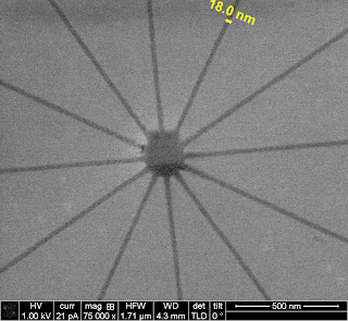 |
| Figure 1. Metal Lift-Off using Gold with a PMMA mask. Line widths are sub 20 nm |
 |
| Figure 2. Metal Lift-off Using Gold with PMMA Mask showing Trench Widths Sub 20 nm |
 |
| Figure 3. AFM Scan of PMMA trench made by E-Beam Exposure |
 |
| Figure 4. Cross Section of PMMA Trench Obtained using High-Resolution AFM Probes |


