On another AFM front I am also spending time trying to locate the 30 nm and smaller lines which is proving to be much more difficult than the 50 nm lines I have posted about before on here. Those lines, which were much more in number creating an array that later proved to be too big for the field size and may have contributed to the lines large widths, were also slightly sloped on the side walls which caused the trench bottom to be smaller than the top (as previously discussed) and made them much easier to find. The new set of e-beam etches were not as sloped and were smaller (which is good!) are much harder to find even with smaller radii AFM tips. So far I have worked with tips down to 1 nm but from literature I have found that without cleaning of the probes the contamination of the tips might be the reason that the lines are so difficult to find (The Journal of Physical Chemistry B, 1998. 102(22): p. 4288-4294. and The Journal of Physical Chemistry C, 2008. 112(38): p. 14902-14906. and The Journal of Physical Chemistry B, 1999. 103(40): p. 8558-8567. to name a few). So once the cleaning procedure has been worked out I can tell if the lines and micelles are hard to image because of the contamination or because my procedure is still lacking. Either way I will update regarding these matters soon!
Wednesday, October 2, 2013
A short update on cleaning and imaging procedures...
Let me be (probably not the first) one to say that if research didn't slog forward it probably wouldn't move at all. I have been working with AFM in attempts to find the right combination of AFM probe and cleaning procedure (of both the substrate and the liquid cell) which will yield micelles on the surface. I have been corresponding with contacts on campus which have experience with cleaning AFM probes (which I have mentioned before can become contaminated by the gel packing which the are stored and shipped in) but once again the difficulty of meshing schedules makes that endeavor a slow one. I am meeting with another research specialist today in hopes of looking at the set up they use and replicating their procedure and apparatus somewhere in our building so that I, and other who are trained to use the AFM, will have access to it so that cleaning of AFM probes will not be such a hassle. I was able to come up with a contamination free way of transporting probes across the university campus which will keep the probes safe, secure and clean following the cleaning, but if I am never able to get assistance in the cleaning then the container is not worth much (although I'm happy that the simple design we came up with works so well).
Friday, September 6, 2013
AFM is a different animal...
Because the SEM technician who runs the microscopy lab at TU has been gone I have shifted focus primarily to imaging micelles on a plain silicon surface. Although for as many papers of it I see it seems like this would be just a sit down at the AFM and get it done in a day or even a few days task, it has proven me wrong. The main issue that I have run across is that working with micelles on the AFM requires a degree of art and a degree of science. After speaking with someone this week who has worked with AFM for some time, although not on surfactants or micelles specifically, I came to realize that you really have to come to know each component that you're using personally. I have tried three tips so far that did not show promise and have moved onto a new set of three which I am hoping will at least point me in the right direction. I have also been in contact with Agilent and Nanosensors.com regarding these subjects and while they are helpful I have come to the conclusion that it will all come down to trial and error with tips and cleaning procedures. It becomes pretty frustrating when I use the AFM for several hours in a day and come away with nothing other than "this wasn't a tip that will do the job" or "that cleaning procedure left too much on the surface". However, there is always another procedure and another tip to try and with free samples from probe manufacturers I have plenty to work with. Once I find "the tip", the plan is to purchase some and coat the backside of a couple with magnetic material which could (has been shown to) increase resolution by decreasing the motion of the solvent (in our case water) by the piezo. A MAC mode nose cone will facilitate this by creating an oscillating magnetic field which will vibrate the tip alone without the piezo.
Another problem which I am dealing with is that most AFM studies done on silicon use a cleaning procedure which leaves the surface hydrophilic, usually by washing in an RCA-1 cleaning solution. For now I am just trying to achieve imaging micelles so I am following this procedure, but my work around in the end is to try a plasma cleaning step on the PMMA layered samples which should leave the exposed silicon in the trenches hydrophilic. The time of the plasma will need to be short in order to prevent damage which could alter the roughness of the exposed surfaces. This week I am trying the PPP-BSI-SPI, the PNP-TR-SPL and the SiNi AFM probes. They are all soft cantilevers (less that .1 N/m and roughly 15 kHz). The problem I have seen with these types of cantilevers so far is that the slightest environmental factor, whether it's air movement from closing the door to the room or sneezing too loudly, causes the cantilever to become erratic. I have developed a few procedural additions which help to lessen their effect and will post on the efficacy of the new tips soon.
Tuesday, July 23, 2013
False Positives
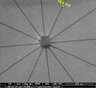
A few weeks ago I was able to travel to Tulsa to try some new E-beam lithography development procedures and the results were very promising. The new procedures, both of which used much shorter development times, were different in that one was at room temperature and the other was at -10 degrees Celsius. The results showed 20 nm trenches and even sub-20 nm trenches in some areas. At first there was some trouble viewing the samples because when they were sputtered with gold and viewed the PMMA shifted heavily and the movement could be seen to happen in real time under the SEM. This lead to the theory that if the V shape, which I have discussed in previous posts, was occurring before the sputter coating then perhaps vertical walled trenches were not having the side walls coated effectively. The samples were brought back to OU and placed in a rotating thermal evaporator and then viewed. The PMMA was motionless, otherwise moved very slowly, and the trenches were small in width as can be seen in Figures 1, 2 and 3 . One side of the wheels were larger than the other which lead me to believe that there may have been a stigmation issue.
However, when trying to replicate the results just recently I saw the larger line widths between 30 and 50 nm that I have gotten in the past, seen in Figure 4.
When discussing with Mr. Nabity he thinks that the wedges of the wheels may have shifted causing one side to be smaller in width than the other and not just a stigmation as I originally thought which is supported by the left side of the wheel being wider than the right, shown in Figure 2. However, because all wheels in the exposure are shifted is seems that it is more than just shifting as I thought if shifting had occurred it would have only been one or two wheels but not all of them. Attempts will continue to improve the resolution and straight wall profile of the trenches but much more focus will be put on imaging micelles using AFM, which is still moving along slowly.
I received some free samples from an AFM probe company and have been trying to coax high resolution images out of them but have been having some difficulty. Part of the problem, I believe, is that all of the literature I have read states that they used cantilevers with very low resonant frequencies and force constants, which makes sense because I am trying to see "soft" things (micelles). However, some of the probes are so flexible is seems that even after centering the laser off of the cantilever onto the photodetector they are prone to drift heavily. Also, the autotune function of the AFM has trouble picking up the low resonant frequencies so manual tuning procedures are going to be done in order to work around this.
Another issue that I have found is that apparently the gel packs in which the AFM tips are stored and shipped cause contamination. I am trying to arrange a way of cleaning the tips in an ozone chamber on campus here at OU and depending on scheduling I am hopeful that I can get this done sometime in the next week!
All in all, still working on the trenches but I believe that they are at a good place where I can start using them for initial results once I can image micelles on the silica surface.
 |
| Figure 1. Trenches developed June 27th using Cold development with shortened time |
 |
| Figure 2. Trenches developed June 27th using Cold development with shortened time |
 |
| Figure 3. Trenches developed June 27th using Cold development with shortened time |
 |
| Figure 4. Trenches developed July 18th using Cold development with shortened time |
Monday, July 1, 2013
Minor Successes Can Lead to Great Victories...(Metal Lift-Off and Hi-Res AFM Probes)
In the world of science I have come to learn that with every small step forward you gain a tool or skill that will make research easier and more efficient in the future. At times I feel like I'm not really moving forward, but then I remember that a marathon is not completed in a single event but many steps. Lately I have had two small victories in the areas of E-beam lithography and AFM. The first is that upon completion of a metal life-off procedure the lines created in the PMMA are actually 20 nm or less! Images of these lift-offs can be seen in Figures 1 and 3. The problem that we continue to battle is that the side walls are not straight up and down vertical but at a slant. At TU last week I used a much shorter development time which lead to the very small metal lift-off lines. When the PMMA was viewed in the SEM, however, it was seen to be continuously pulling away (trenches were widening) due to beam damage.
This raises the question of whether or not we have actually been reaching the small line widths before and the SEM viewing was distorting the PMMA or if they were wide and then viewed. I believe the latter to be true because this was the first instance where the PMMA was seen to be actively moving under the electron beam, whereas before it had already moved and was then viewed. I think that the longer development times overdeveloped the walls, causing the slant, which were then viewed under SEM and did not move because they had already reached their "equilibrium" position. So when the development time was shortened only the exposed area was developed and upon viewing the PMMA began shifting to its equilibrium position and we were able to see it.
Another question that arises is how it the beam damage occurring if we are sputtering with gold? Two possibilities is that the gold layer is not thick enough (roughly 2.5 nm on the surface may not be enough to negate the effects of the beam) or perhaps the side walls of the trench were not coated because they were straight up and down. If this were the case if could also explain why the overdeveloped slanted walls did not move when viewed. Because they were already slanted the gold formed a layer there which could have helped protect against beam damage. The straight vertical walls may not be coated as well and therefore when viewed under SEM they are not protected and experience the beam damage. This theory will be checked using a rotating thermal evaporator in an attempt to coat the side walls of an un-viewed sample, and it will then be viewed to see if the same damaged and extreme movement occurs again.
The second small victory is the use of high-resolution AFM probes in order to see the bottom of one of our trenches and make a more accurate measurement. The cross sectional view of such a trench can be seen in Figure 4. As compared with the last post in which the trench was roughly measured as 300 nm across and "V" shaped, this new measurement shows a trench with a square bottom. The slanted walls are still present, and show some tip-sample interaction on the left side of the cross section which is still being investigated, but the sample bottom appears to be roughly 58 nm across. The sample used was an older one with many doses being tested and it is difficult to know which dosage this was but due to the recent success with the metal lift-off procedure a usable dosage is much more easily identified.
The next goal is to obtain micelle images on a silicon surface using high-resolution AFM probes, along with the work being done to check how vertical the walls of the trenches are and perhaps obtain an image of them using SEM if possible.
 |
| Figure 1. Metal Lift-Off using Gold with a PMMA mask. Line widths are sub 20 nm |
 |
| Figure 2. Metal Lift-off Using Gold with PMMA Mask showing Trench Widths Sub 20 nm |
 |
| Figure 3. AFM Scan of PMMA trench made by E-Beam Exposure |
 |
| Figure 4. Cross Section of PMMA Trench Obtained using High-Resolution AFM Probes |
Wednesday, June 12, 2013
Partial Success Using AFM to Find EBL Patterns but More Work Needed
Over the past two months I was ill and had finals for school and was not able to go to Tulsa for EBL as often as I wanted to but I will update with what I have. When going on some of the images given to me by the group who was able to reach ~20 nm lines I noticed that their trenches were not totally straight up and down, as seen in Figure 1. I was able to travel to travel to Tulsa to perform some exposures and noticed that even though I do not have cross sectional images there does seem to be a wide opening of the trench at the top (PMMA surface) and a smaller line width at the bottom of the trench (substrate surface). Figures 2 and 3 show the phenomenon that I am discussing, and upon correspondence with Mr. Joe Nabity, the creator of the EBL system we are using, he agreed with my conclusion that there seems to be a V shape to the trench. The tops of the trenches appear to be between 40 nm and 70 nm on average while the trench bottoms appear to be anywhere from 10nm to 20 nm (although it is difficult to confirm this without first performing a metal liftoff which we will do next visit to TU). The reason for using EBL in PMMA was that straight up and down walled trenches have been obtained using it and a "V" shape may introduce prevent adequate confinement of the surfactant molecules which we are attempting to observe using AFM. The time spent on this project is becoming lengthy and therefore in the interest of moving forward we will be making a sample to use with AFM. The sample will most likely display the small trench bottom and have a large trench opening but will provide a way of working on a method for imaging surfactant aggregates at the bottom of this trench while also working on fixing the problem of the "V" shape. I have contacted several corresponding authors of publications which have been able to obtain the types of line widths we are looking for while also keeping the trench wall vertical. A few of the papers are Systematic study of the interdependence of exposure and development conditions and kinetic modelling for optimizing low-energy electron beam nanolithography (Mohammad) and Fundamentals of Electron Beam Exposure and Development (Stepanova).
I have also been doing AFM on some of the previous samples I have made using EBL. They have a layer of gold roughly 20 nm thick with a pattern called Line Dose Test which had 56 sets of lines with line widths between 40 and 60 nm. Figures 4 and 5 show an AFM and SEM image of one of the lines with an unknown location in the array of lines, due to the nature of AFM. Being able to find these lines is a feat in itself but I've been able to do it several times now on the same sample, even in liquid! Because the AFM tip is roughly 90 nm we have not been able to obtain data on the trench bottom but high-resolution tips (smaller tip radius) have been ordered and will be used in further experiments. Another observation made is that the AFM showed a line width of roughly 300 nm, seen in Figure 7, which according to the SEM micrograph of the same sample in Figure 6 is not accurate. One possible explanation is that the PMMA has contracted over time leading to a wider trench opening that previous seen, and this possibility will be checked using SEM once again. Another possibility is that the PMMA is elastic enough that the AFM tip is dragging the top edge of the trench as it scans along and it snaps back to its original width as the AFM tip moves past. I feel that this is unlikely as the PMMA is layered in gold which should be thick enough to hold it PMMA in place, but this would able contradict the explanation of the PMMA contracting. We will perform AFM with the new tips to see if the same phenomenon occurs and explore it further if it continues.
I have also been doing AFM on some of the previous samples I have made using EBL. They have a layer of gold roughly 20 nm thick with a pattern called Line Dose Test which had 56 sets of lines with line widths between 40 and 60 nm. Figures 4 and 5 show an AFM and SEM image of one of the lines with an unknown location in the array of lines, due to the nature of AFM. Being able to find these lines is a feat in itself but I've been able to do it several times now on the same sample, even in liquid! Because the AFM tip is roughly 90 nm we have not been able to obtain data on the trench bottom but high-resolution tips (smaller tip radius) have been ordered and will be used in further experiments. Another observation made is that the AFM showed a line width of roughly 300 nm, seen in Figure 7, which according to the SEM micrograph of the same sample in Figure 6 is not accurate. One possible explanation is that the PMMA has contracted over time leading to a wider trench opening that previous seen, and this possibility will be checked using SEM once again. Another possibility is that the PMMA is elastic enough that the AFM tip is dragging the top edge of the trench as it scans along and it snaps back to its original width as the AFM tip moves past. I feel that this is unlikely as the PMMA is layered in gold which should be thick enough to hold it PMMA in place, but this would able contradict the explanation of the PMMA contracting. We will perform AFM with the new tips to see if the same phenomenon occurs and explore it further if it continues.
 |
| Figure 1. V shape seen by previous group |
 |
| Figure 2. Plan view image of exposures showing wide trench opening and narrow trench bottom |
 |
| Figure 3. Plan view image of exposure showing wide trench opening and a slant to narrow trench bottom |
 |
| Figure 4. AFM image of Line Dose Test Exposure |
 |
| Figure 5. SEM micrograph of Line Dose Test exposure |
 |
| Figure 6. Line Dose Test Line Width via SEM micrograph |
 |
| Figure 7. Line width of Line Dose Test Line via AFM metrology |
Friday, April 12, 2013
Cold E-Beam Development and Magnification Transition Values
It has been a slow time for the last few months as classes have been exceedingly time consuming this semester. I have made two trips to Tulsa after doing some research on the use of cold developer in order to improve line resolution. The developer MIBK:IPA and the post development rinse of pure IPA were chilled in a freezer to -15 degrees Celsius prior to the development process. The theory behind the development process is that the e-beam process causes long chain "scission" where the polymer is exposed. The main areas of exposure have longer chains and are more soluble, while the areas near by the main area of exposure still have scission but they are shorter, mostly caused by secondary and backscattered electrons. The longer the chains are the more soluble they are, but as the temperature of the developer is raised the shorter chains become more soluble as well. By lowering the temperature the shorter chains are made more insoluble and therefore the line width will increase in resolution. Below are images which show development at room temperature (RT) and at -15 degrees Celsius. Development in both cases was done for 30 seconds in both the developer and the post rinse.
The cold development definitely showed a difference between 60 nm and 30 nm at the same dosage. There was a slight tilt to the sample that was not known until post etch which may have affected some of the etching but the resolution of both lines suggests that this was probably not the case.
Another test was run at -15 degrees Celsius which showed similar results, but even after decreasing the current to 5.6 pA the line width did not decrease as was expected, but remained the same.
It was at this point that Joe Nabity, the designer of the system being used in Tulsa, was called (instead of just email correspondence) and our problem was shared with him. Mr. Nabity made us aware of a design parameter called the "magnification transition value", which is a magnification where the microscope must change between to relays or circuits. Being on the low end of the range can decrease resolution by a factor of two and therefore not accounting for this parameter may be the reason for our bigger line widths. On the next visit I will be determining the magnification transition value for the working distance, accelerating voltage and operating current. Then by knowing this value we can perform an etching just slightly above it and below it in order to see if this makes a difference. The pattern being used will need to be changed as well in order to make sure it fits in the magnification field. The pattern we have been using has a maximum magnification of 786x, which I believe is too small and therefore if we increase the magnification then the pattern will need to decrease in size in order to fit. The results of this trial should be ready by next week. Mr. Nabity has informed me that if this does not fix the issue then it is something more subtle.
 |
| E-Beam Lithography with PMMA on Silica- 2.00 nC/cm2 dose, 30 kV and 29 pA current, development performed at -15 degrees Celsius |
 |
| E-Beam Lithography with PMMA on Silica- 2.00 nC/cm2 dose, 30 kV and 29 pA current, development performed at RT (25 degrees Celsius) |
The cold development definitely showed a difference between 60 nm and 30 nm at the same dosage. There was a slight tilt to the sample that was not known until post etch which may have affected some of the etching but the resolution of both lines suggests that this was probably not the case.
Another test was run at -15 degrees Celsius which showed similar results, but even after decreasing the current to 5.6 pA the line width did not decrease as was expected, but remained the same.
 |
| E-Beam Lithography with PMMA on Silica- 2.00 nC/cm2 dose, 30 kV and 5.6 pA current, development performed at -15 degrees Celsius |
Wednesday, February 20, 2013
20 nm lines and Smaller but Lacking Consistency
It has been a busy couple of weeks but mostly in preparation of events which come and go very quickly. About 3 weeks ago (I have been quite busy and at one point decided to wait to see if I could improve the results prior to posting but the technician was out of town) I saw lines that were 20 nm and less in width, which are seen in Figures . However, I was unable to consistently achieve these line widths and in the end they seem more like happy coincidences than planned results. They reason I say this that the smaller lines appear on a small pattern located within another pattern which does not display the same line widths. I have been using the wheel arrays for some time to try and obtain smaller line widths and they have served their purpose very well up to this point but now I am stuck at 40-45 nm consistently and I thought it might have something to do with a curving line compared to a straight line. The 40-45 nm results are a big improvement over where I began and with each visit I am fine tuning the procedure but I feel that a small something is missing that is necessary for making these lines smaller. I have been in contact with the manufacturer of the e-beam set up being used in Tulsa and he has given many suggestions of why we haven't been getting the finest lines possible and it is his advice which I will be following up on Friday. With the help of a research scientist here at OU I have been using a new pattern which is a set of straight lines which I felt might give an idea if the curve in the lines was what was causing the large line widths. As seen in Figures , the pattern worked very well, which I was a little surprised about since it was my first custom pattern where I input new current dosages and ran it from scratch, but the line widths still hover close to 40 nm at the lowest line dosages used in the dosage array. As the dosage is increased the sharpness of the line is greater but the line widths also increase. This is expected and what we would want to find is a "sweet spot" where the resolution of the line is greatest while also giving the smallest line widths, which is what I'm hoping will occur on Friday when I go to try out the suggestions of the manufacturer. Until I am able to figure out the problem I have been working with AFM to get images of surfactant on the surface of my substrate, but it is more difficult that one initially thinks. It is a very delicate process but I believe that I am slowly getting the hang of it and hope to have some images soon!
On the terraces fore front things are not going as well. I have been trying to contact the research scientist who has been helping me to obtain the pillars via Reactive Ion Etching but I have so far been un-successful. The main problem occurring is that some of the equipment is in need of repair and the technician helping me was gone for a couple weeks for research and had not been able to fix it the last time I spoke with him. So in the mean time I have been working on protocols to use and trying to fine tune the parameters in order to get the cleanest etch with highest aspect ratio. I am hoping that the issues will be resolved soon and I will be able to continue with the project in it's entirety.
All in all I'd say that for a short while everything was working and moving forward and now once again I am at a veritable standstill. However, I am seeing improved imaging of surfactants on silicon which is keeping me busy while I wait for the etching equipment to be fixed, while preparing for the time when 20 nm lines are reached, which I have a feeling is going to be very soon!!
 |
| Figure 1. Etched 15 nm lines in PMMA on Silicon |
 |
| Figure 2. Etched 20 nm lines in PMMA on Silicon |
 |
| Figure 2. Etched 20 nm lines in PMMA on Silicon |
 |
| Figure 3. Etched 20 nm lines in PMMA on Silicon |
 |
| Figure 4. Etched 20 nm lines in PMMA on Silicon |
 |
| Figure 5. 40 nm lines at the lowest current in a custom straight line array |
 |
| Figure 6. 90 nm lines achieved at highest dosage in straight line array |
 |
| Figure 7. Image showing the entirety of one straight line array which ranges from 1 nC/cm to 8 nC/cm. Etching in PMMA on Silicon using E-Beam Lithography |
Tuesday, January 15, 2013
Polystyrene Bead Etching and E-beam Optimization
It has been some time since I have posted, mainly due to holidays and equipment malfunctions but I have new images and new plans to report! On the pillar or "trough" side of the project we have successfully completed an etching trial which displayed some interesting results. Five samples of 100 nm polystyrene beads on silicon were run under different conditions using CF4 and O2 etching. From figures 1 through 5 below, it can be seen that there was some etching of the silicon and in a few instances there were cylindrical formations, but the beads are being etched by the O2 which causes them to either adhere to the silicon and melt, which causes the final structure to be malformed, or as the bead is eaten it shrinks causing a cone or rounded shape hemisphere shape. From literature I am finding that shorter etching times with higher power (W) seems to give more anisotropic etching profiles (following performance optimization) and the use of a passivation step (usually flowing a polymer) was used in some, but not all, cases. It seemed though that in some of the cases that a reactor had been specially ordered or built for such etching and may not be feasible for our purposes because alternative means of achieving near comparable results are possible. Our next step may be to shorten the etching time for each pulse from 45-60 seconds to somewhere around 5-15 seconds to allow the sample to cool. Also, in the literature the lowest power used in the RIE (reactive ion etching) step was 600 W and we use at the most 60 W and I am interested to see if we increased the power and shortened the pulse time if our etch might become more anisotropic. We will also have to use a different plasma (perhaps argon) and remove all O2 etching steps as they degrade the beads quickly.
The other side of the project is the "trench" or "trough" formation in PMMA using e-beam lithography. After a few setbacks (new source installation and a cooling pump break down) I was able to return and etch a few samples to continue to try and achieve 20 nm lines. So far I can get 50 nm almost every time and still have a few things that I can adjust to see if they shrink that number a bit. Some of the most recent images can be seen in figures 6, 7 and 8. Next I will try to reduce the scope current and see if a smaller dosage per length might help reduce the beam interaction with the sample, creating a smaller line width overall.
 |
| Figure 1. Polystyrene Bead Etching on Silica |
 |
| Figure 2. Polystyrene Bead Etching on Silica |
 |
| Figure 3. Polystyrene Bead Etching on Silica |
 |
| Figure 4. Polystyrene Bead Etching on Silica |
 |
| Figure 5. Polystyrene Bead Etching on Silica |
 |
| Figure 6. Line width of e-beam wheel on PMMA |
 |
| Figure 7. Line width of e-beam wheel on PMMA |
 |
| Figure 8. Wheel Array with Different dosage per wheel |
Subscribe to:
Posts (Atom)